
When you start to experiment with radio frequency circuits and projects one of the tools that is a must have is a RF signal generator. Sometimes you want to test the response of a filter and need to sweep through a range of frequencies or need to generate a carrier or clock frequency. Having a signal generator could be invaluable for these types of experiments and projects. The problem is that these devices are normally not cheap and most makers and hobbyists just can’t afford to buy expensive signal generators that can produce signals in the GHz range. Recently I noticed a number of people rolling their own by either using a chip from Analog Devices that goes up to 4.4GHz or one from Maxim which goes even higher up to 6GHz.
So in this post I will discuss my attempt (and work in progress) at building a RF signal generator that can generate signals from 35MHz up to 4.4GHz. It will do this with 1kHz frequency resolution and adjustable output power levels. At the heart of this generator will be the ADF4351 synthesizer chip from Analog Devices. It achieves this wide band signal generation by using a phase locked loop (PLL) with a reference oscillator and number of divider circuits. If you are a bit rusty on PLL’s I will quickly explain the basics since it will help to understand how to program this chip later.
Phase Locked Loop
In a typical PLL there are 3 critical parts: the voltage controlled oscillator, the phase comparator or detector and the loop filter.
VCO
The voltage controlled oscillator (VCO) takes an input voltage and outputs a frequency that depends on that input voltage. In other words by changing the input voltage we can adjust the output frequency of the VCO. So in theory if we wanted to build a signal generator we could just program a digital to analog converter to set a voltage on the VCO input and on the output we would have our signal. This should work but it would be an open loop system and the output signal would not be very stable. The problem is that small voltage changes on the VCO input can have fairly large changes in the frequency of the output signal and we have no way of automatically correcting any error. To fix this we need to have a closed loop system that would constantly adjust the VCO voltage to keep the output signal frequency constant. This is where the next two parts fit in.
Phase comparator/detector
The phase comparator take two input signals and, as it’s name suggests, compares them to produces an output voltage that is proportional to the phase difference of the two input signals at any time. So if the instantaneous phase of the two signals are the same it would produce a constant voltage and if not it produces a higher or lower voltage. Since we know that two signals which always stays in phase must have the same frequency it means that the two frequencies are compared.
Loop filter
The last part of the PLL is the loop filter. The purpose of this filter is to remove any noise and high frequency components that could have been generated by the phase comparator. It also helps to improve the response of the VCO by for example dampening the phase comparator output to prevent overshoot or oscillations when there is sudden changes in frequency. Keeping the bandwidth of this filter low produces a steadier output frequency but will also increase the time needed to change the frequency. If your application needs quick frequency changes then a wider bandwidth filter would be better.
Now if we connect the parts together and add a reference signal we get a nice closed loop system that produces a very stable VCO output frequency.
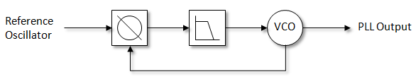
When we switch this circuit on the phase comparator will produce a large output voltage since initially the second input is 0Hz. As the VCO starts to kick in and it’s output frequency increases, the phase comparator voltage will decrease. When the two frequencies match, the phase comparator output voltage stabilizes and the loop is said to be locked. In the locked state this PLL will then output the exact same frequency as the reference input.
This is all good and well but after all this we still only have the reference frequency! Are we not suppose to build a signal generator that can generated signals of various frequencies! Just read on, we will get to that part next.
Synthesizer
Imagine we could place a circuit in the VCO feedback path which would divide the frequency by a given number, say for example 2. The phase comparator would then increase it’s output to the loop filter and VCO until it’s two inputs match again. Since in this example we divided the feedback by 2, it means the phase comparator will drive the VCO to output a signal 2x the reference frequency. If our reference was 10MHz then the VCO would now output 20MHz.
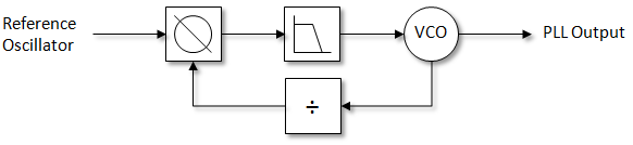
As you can see, by adjusting the division in the VCO feedback path we can adjust the output frequency. This is basically how an Integer-N PLL Synthesizer works.
One thing you might have noticed is that the output will always be an integer multiple of the reference frequency. So if you have a 10MHz reference you would only be able to generate 10MHz, 20MHz, 30MHz, etc. To solve this many manufacturers of PLL devices also allows fractions of the reference to be used. These types are known as Fractional-N PLL Synthesizers. Furthermore, you will also notice that in addition to the divider circuit in the VCO feedback path, many devices also adds dividers on the reference frequency input and on the VCO output. By tuning all these different dividers one can generate a large variety of frequencies within the device’s range.
Back to the generator
As mentioned in the introduction we will be using the ADF4351 Fractional-N Synthesizer chip for our RF signal generator. Now this is a really great device but it still needs a couple of supporting components. Things like the loop filter circuit and a reference oscillator still needs to be added and then there is PCB layout considerations when working with VHF and UHF frequencies. These are all things that could slow down the project if we tried to build it from scratch. Luckily for us some breakout or evaluation boards are cheaply available online which has all these things covered. There are various versions of these boards but the one I used is build on a black PCB as in the photo below:

I bought this one more than a year ago and can’t remember the exact price but normally they go for about $20.
In addition to the ADF4351 the board also contains:
- 25MHz TCXO (Temperature Compensate Crystal Oscillator) reference oscillator
- small linear voltage regulator (as the ADF4351 is a 3.3V device)
- loop filter circuit
- fundamental and compliment RF outputs on SMA connectors
- external reference oscillator input on SMA connector
- SPI and a few other pins broken out to a 2×5 0.1″ header connector
This covers most things and all we need now is a microcontroller to drive this board.
Microcontroller
The chip provides a SPI interface to configure it’s six 32bit registers. So basically all that the microcontroller should do is to calculate these register values and write them. This means we could use just about any MCU and the popular options would be to use an Arduino Uno or Nano. In my case I decided on the STM32F103 and in particular the “Blue Pill” board that I reviewed here. The reason for this is that it’s already a 3.3V device (so no level translation is needed on the SPI pins) and I plan to add some features in the future which might take advantage of the faster processor and extra memory. Another added bonus is that the STM32duino framework uses 64bit double variable types compared to 32bit doubles used by the normal framework. This comes in real handy when having to hold numbers like 4300000000Hz (or 4.3GHz) where a 32bit unsigned integer just falls short at a maximum of 4 294 967 296. This does not mean that you can’t build this project with the normal Arduino framework, it just would take some extra planning to handle large numbers or high precision small numbers.
Wiring it all up
I wired the SPI pins of the STM32 board to the ADF4351 board like in the table below:
| Pin Function | STM32 Board | ADF4351 Board |
| Load Enable | PA4 | LE |
| SPI Clock | PA5 | CLK |
| SPI MOSI | PA7 | DAT |
| Lock Detect | PB0 | LD |
For programming and interfacing my PC with the MCU I connected a small USB to serial adapter board to pins PA9 and PA10 (which is UART1 for this MCU). This adapter board then also provides a 5V output from the USB port which is used to power both of the boards.
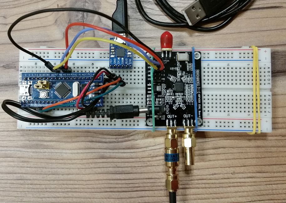
When the RF power is switched on both output ports (OUT+ and OUT-) will output the signal but just with a 180° phase difference. To prevent having an open connection that would reflect the energy back to the device I terminated one of the outputs with a 50ohm dummy load. On the the output that I am using I placed a fixed 10dB attenuator just to protect the spectrum analyzer a bit incase something went wrong.
Programming the ADF4351
As mentioned before, the chip has six 32bit registers that is programmed via it’s SPI interface. It only has an input (MOSI) called DATA, a clock (CLK) input and a chip select (LE) input so we can only write to the registers. The order in which the registers are programmed are also important and should be from register 5 through to register 0.
While programming the chip registers it helps to have a good understanding of how all it’s different parts fit together, therefore I added the block diagram provided in the datasheet (which you should anyway also read in combination with this post) below:

As you can see there are a couple more blocks than the simple synthesizer diagram we looked at earlier, but still not rocket science. Some interesting things to note is that on the reference input (top left corner) there are also some doubler, divider and counter blocks. These allow us pretty fine control over the reference frequency which reaches the phase comparator. We can also see that pin CPout feeds the external loop filter and provides the voltage back to pin Vtune which feeds the VCO. From the VCO we see the feedback path through the divider circuit and back into the phase comparator. Then there is also the VCO output to another set of dividers just before the final output stage.
This last set of dividers are actually also very important since the VCO of the chip can only output frequencies between 2.2GHz and 4.4GHz. So if we want to output lower frequency signals we would need to use these dividers in our calculations. Something to also keep in mind is that the VCO on the chip is actually build from 3 different VCO’s which have overlapping frequency ranges. Luckily for us the selection of which of these VCO’s to use is mostly handled automatically, and needs very little input from our side.
Calculate the frequency
When setting the output frequency we would need to calculate values for the divider on the feedback path between the VCO and phase comparator and also on the output dividers just before the RF output. The divider on the feedback path consists of 3 values: the integer (INT) value, the fractional (FRAC) value and the modulus value (MOD).
RF Divider
Typically we start with the output divider value, as an example lets use an output frequency of 433MHz. We know that the VCO operates only between 2.2GHz and 4.4GHz so we have to select a divider value which will put our wanted frequency in the VCO output range. In this case an output divider of 8 would work, since this would put the VCO output range from 2.2GHz / 8 = 275MHz to 4.4GHz / 8 = 550MHz. If we are going to divide the VCO RF output by 8 to get our wanted frequency then it means we would also need to make sure the VCO generates a frequency 8 times higher than our wanted frequency. So the VCO output frequency we would aim for would be 433MHz x 8 = 3464MHz.
INT, MOD and FRAC
To get this VCO frequency we need to find values for the feedback path divider. The first one would be the integer value, which is pretty easy since we talked about it earlier. All we need to do is take the wanted VCO frequency divide by the reference oscillator input. Let’s say in this case it’s a 25MHz reference then the integer value would be 3464MHz / 25MHz = 138.56 and since it’s an integer we only take 138. Next we need the modulus which we calculate by taking the reference oscillator divided by the smallest frequency resolution we would need. Lets say 100kHz resolution which will give us a modulus of 25MHz / 100kHz = 250. Finally we calculate the fractional part by multiplying the modulus with the fractions that we lost during the integer calculation which gives (138.56 – 138) * 250 = 140. If you wanted to optimize these last two values you could also look for the common denominator which would be 10 and would make the modulus 25 and the fraction 14.
Frequency resolution
Something to note about the resolution is that the modulus is stored in 12bit space which means the smallest fraction we can represent is 1/4096 multiplied by the reference frequency. In the example above we used 25MHz which would give a resolution of about 1/4096 * 25MHz = 6.103kHz. In the beginning of this post we mentioned a 1kHz resolution, so how do we get it. Since we can not change the modulus size all that’s left to change is the reference frequency. Here we have two options, physically replace the oscillator with a lower frequency one or we use the reference oscillator counter to divide it down. If you look back at the block diagram you will notice the “10-BIT R-COUNTER” block between the reference input and the phase comparator. If we use this counter to divide by 8 we have a new reference of 25MHz / 8 = 3.125MHz which would now give a frequency resolution of 1/4096 * 3.125MHz = 763Hz. So as we can see, by dividing the reference frequency down to a lower value we can increase the output resolution.
One last catch, remember earlier we spoke about the VCO that actually consists of 3 VCO’s operating in different bands but which is automatically selected for us. Well the R-Counter also clocks this automatic circuitry and by changing the R-Counter we also adjust it’s clock which should stay below 125kHz. This clock can be adjusted to stay below the 125kHz limit by updating the BandSelectDivider bits, for me using 200 / R-Counter worked well.
Armed with the calculated values, we can now set our desired frequency by writing them to the relevant registers. As a tip, Analog Devices also provides a small program that you can download from their site to help calculate registe values. Initially it is very helpfull and is highly recommended to verify your register values against but later you would anyway need to learn how to calculate the values yourself.
Output power level
The chip allows us to change the output power in 3dB steps from -4dBm up to 5dBm by writing to the relevant bits in register 4. The absolute accuracy of the output power depends on the board layout and components used. On the tests I performed I got about 5dB less on the absolute levels but the relative levels were very close. Below about 1.4GHz the absolute level seems fairly stable and within 1dB but higher up it started to fluctuate up to about 5dB higher and lower.
Building the signal generator
After wiring the STM32 and the ADF4351 board together I wrote a small library for the ADF4351 which more or less performs the tasks we talked about in the above sections. I also wrote a basic command line interface that allow me to set the frequency, power etc. This interface is based on SCPI which is the Standard Commands for Programmable Instruments. The commands are ASCII based so can be easily send from a terminal program. I have also added some extra features like sweeping over a frequency range which would be very usefull when testing the frequency response of a device under tests. A very basic working version of the source code can be downloaded here: SignalGen(22-12-2018).
Using the signal generator
After flashing the code the signal generator can be controlled by sending it commands via UART1. The commands that are currently implemented are all in group SOURCE and shown below.
| Task | Command | Example |
| Set the frequency | :SOURCE:FREQ | :SOURCE:FREQ 433000000 |
| Set the power level | :SOURCE:PWR | :SOURCE:PWR 0 |
| Enable/disable RF output | :SOURCE:RFON | :SOURCE:RFON 1 |
| Check if PLL is locked | :SOURCE:FREQLOCK? | :SOURCE:FREQLOCK? |
| Set sweep start frequency | :SOURCE:SWEEPSTART | :SOURCE:SWEEPSTART 35000000 |
| Set sweep stop frequnecy | :SOURCE:SWEEPSTOP | :SOURCE:SWEEPSTOP 4400000000 |
| Start/stop sweep | :SOURCE:SWEEP | :SOURCE:SWEEP 1 |
As I progress with the project I will add new commands and also improve the command line interface to comply more with the SCPI standard.
So how good is it?
Well concidering what it cost us to build this basic signal generator it’s not that bad. Depending on what you want to do with it, it might be perfect for the job.
Harmonics
The output signal has some pretty strong harmonics on the lower frequencies which might be due to the dividers. Generating signals between 2.2GHz and 4.4GHz the power in the harmonics seems lower, which could confirm our idea that the dividers causes more squarish waves. Below is a trace of a 100MHz signal and it’s odd harmonics:
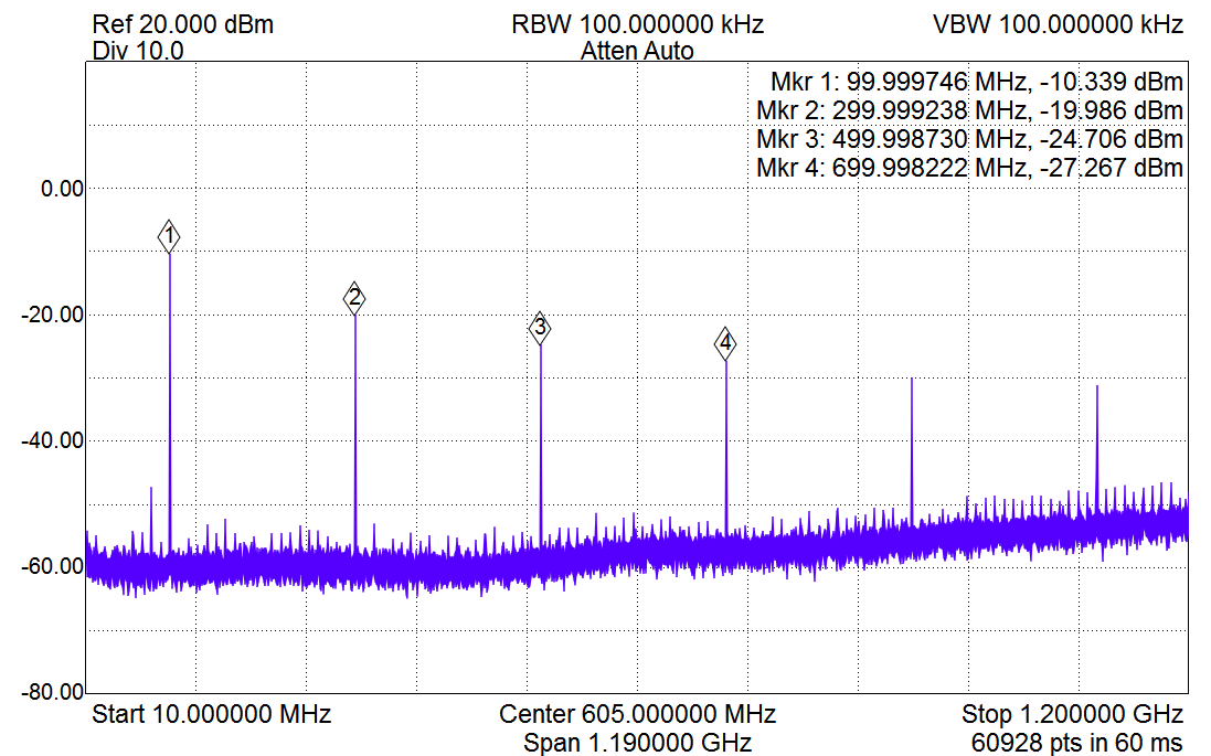
So as we have said, some pretty strong harmonics. But I have read that some people actually take advantage of these harmonics to get signals at frequencies far beyond the range of the device. If for example you needed a 8GHz signal then you could tune to 4GHz and use the second harmonic.
Frequency stability
On the frequency stability side it also performs okay. It helps to give the oscillator a couple of minutes to warm up if you want to increase the accuracy a bit. It seems the TCXO’s on these boards has a frequency tolerance of about 20ppm to 50ppm which starts to show on the higher frequencies. To compensate for this I checked the frequency error (assuming my spectrum analyzer is correct) at a couple of frequencies and calculated a ppm value. The value came out at around the expected 20ppm which I then applied to the reference frequency in the calculations. This seems to work pretty well and most signals are now very close to the desired frequency. In the trace below I allow a couple of minutes for warming up and then tuned to 500MHz:
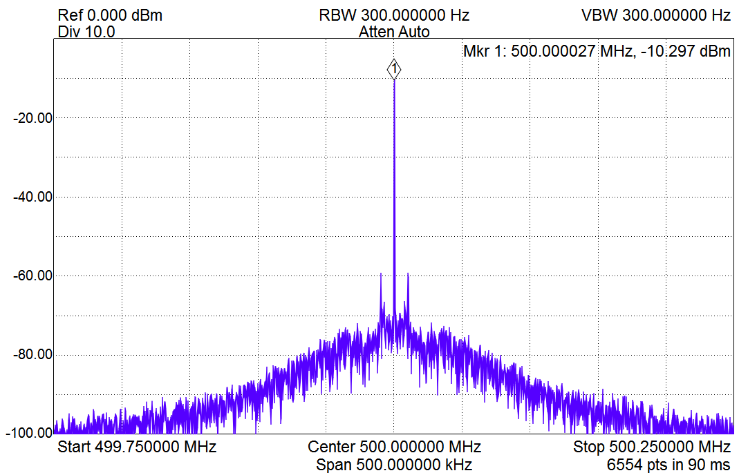 Just 27Hz error (again assuming the spectrum analyzer is perfect). Not bad, but I noticed that slight temperature changes like blowing over the oscillator can cause the frequency to change a bit.
Phase noise
Unfortunately my spectrum analyzer can’t measure phase noise, but you can make your own crude estimations from the 500MHz trace above. If I have to estimate it looks a bit worce than the values provided in the datasheet (-114dBc/Hz at 100kHz) but it’s still not that bad and again depends on your application. One thing I have read is that a better power supply could also improve the phase noise and is something I will try in the future.
Spurious emissions
We can see two spurs, one on each side of the 500MHz plot. With my configuration I have actually not noted a lot of other spurious emissions.
Output power
As mentioned earlier the levels are a fair bit lower than the chip specifications and also not so constant at higher frequencies, but this could all be due to the board. Below I have made two maximum hold sweeps, one at the maximum power and one at the minimum power.
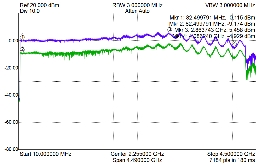
We can see that the relative power levels looks fine with a 9dB difference between the two but the absolute levels are not on par.
Conclusion
All in all I am very happy with the project and performance of the ADF4351 (running on this low cost board) and it pretty much do what I wanted it to do. If you wanted to use this as a signal source for sweeping a filter it would be perfect. But if you wanted to use it to generate a test carrier signal that you will be transmitting into space then you might want to add some additional filtering to get rid of the harmonics.
What’s next
This is a good start but there are still a lot we can do to improve this signal generator. Some of these things and other fun experiments include:
- Add a filter bank on the output to try and supress the harmonics.
- Use a more accurate reference frequency oscillator.
- Add an amplifier and adjustable attenuator to allow a larger range of output powers.
- Add LCD and external controls to allow the signal generator to be used without a PC, maybe also add a battery pack.
- Make a nice enclosure for it.
- Add a RF power detector to add some scaler network analyser features.
- Improve and optimize the code.
- Experiment with a modulation input to perform Direct Digital Modulation to create FSK modulated signals.