
Whenever I reach for the ATTiny85 I usually just use Arduino to program it, meaning the Arduino IDE and libraries. But the other day I was glancing over its datasheet and realized again how relatively simple this microcontroller is. So how hard could it be to shave off some layers of abstraction and get down to the bare metal on it. Well lets see how low we can go!
What you will need
To follow along you would need a text editor, it could be as simple as notepad, although I would rather go for something a bit more powerful like Visual Studio Code. You would also require a cross compiler, I used the XC8 compiler from Microchip which you can download for free from here. Then you would furthermore need a programmer and some software to upload the program to the ATTiny85 with. As programmer I use the USBtinyISP which can be cheaply found on ebay or other maker stores.
In combination with the USBtinyISP programmer I used AVRdude. AVRdude can be downloaded from SourceForge but I have recently heard a lot of complaints from people downloading it from there, so just be careful. Since it comes packaged with Arduino I just use it from there and did not download it. Another possible source to try if you need to download it is from here.
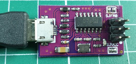
Oh and then of course you would need an ATTiny85. If you have some kind of development board you could try it or just build a basic circuit on a breadboard. Something like this should do:

The pin out of the ATTiny85:

So in the test circuit we have power (5V) and ground on pins 8 and 4 respectively and on pin 5 (PB0) a 1k resistor and LED. The rest of the connected pins goes to the USBtinyISP programmer. The ATTiny85 is powered by the programmer in this case.
Now would also be a good time to make sure that you have a copy of the ATTiny85 datasheet downloaded.
Setting things up
To keep things a bit organized I often use a simple folder structure which has the project folder at the root with at least a nested “src” and “output” folder. The “src” folder contains the source code and the “output” folder all the output created during the build process. So something like this:

Then in the root I also create three batch files named “build.bat”, “flash.bat” and “writeFuses.bat” and as their names suggest are used for building the source, flashing the program and writing the fuses to the microcontroller.
The “build.bat” file has the following contents:
SET PATH=%PATH%;E:\Programs\Microchip\xc8\v2.31\bin
CLS

xc8-cc.exe -mcpu=attiny85 -std=c99 -mext=cci -o output\test.elf src\main.c
xc8-cc.exe -mcpu=attiny85 -std=c99 -mext=cci -S -o output\test.s src\main.c
avr-objcopy.exe -O ihex output\test.elf output\test.hex

pause
The first line adds the compiler’s bin folder to the PATH environment variable. This is done so that we can call the compiler from any folder. Depending on where you installed XC8 your path could look a bit different. Note that the PATH environment variable is only set for this session of the batch file. The second line just clears the screen to remove any previous messages.
Then in the third line we call the compiler with some options:
-mcpu=attiny85
Just tells the compiler which CPU we will be using.
-std=c99
Tells the compiler that our code will conform to the C99 standard.
-mext=cci
This enables the CCI (Common C Interface) language extension used by XC compilers. This will allow us to use the build in compiler support for handling interrupts.
-o
Tells the compiler to output an .ELF file in our output folder.
Then in the next line we make the same call but this time add the -S option and change the output file extension to .s. What this does is to compile our program also to assembler. This step is not important for creating the files we need for programming the ATTiny85 but it does give us a “behind the scenes” view of our C coded program.
In the next line we use “avr-objcopy.exe” to generate a hex file, which is what we need to program the microcontroller with.
The last line just cause the command window to stay open until we press a key. This allow us to see if any errors were generated during the build process.
The “flash.bat” file has the following contents:
SET PATH=%PATH%;C:\Program Files (x86)\Arduino\hardware\tools\avr\bin
CLS

avrdude.exe -C "C:\Program Files (x86)\Arduino\hardware\tools\avr\etc\avrdude.conf" -v -p attiny85 -c usbtiny -U flash:w:output\test.hex:i

pause
As before the first line temporarily modifies the PATH environment variable, this time it adds the path to avrdude. As I mentioned before I am actually using it from the Arduino installation. So just double check your path and if needed modify it to point to your instance of “avrdude.exe”.
The following line just clears the screen again.
The third line calls “avrdude.exe” with the following options:
-C “C:\Program Files (x86)\Arduino\hardware\tools\avr\etc\avrdude.conf”
Provide the location of the configuration file, in this case it is also located in the Arduino folders. Yours might be different if you installed avrdude separately.
-v
Enable verbose output.
-p attiny85
Specify the part number of the device we want to program.
-c usbtiny
Specify the programmer that will be used, in our case the USBtinyISP programmer.
-U flash:w:output\test.hex:i
Specifies the memory operation we want to do. In this case we want to operate on “flash” writing, “:w”, “output\test.hex” which is in Intel hex, “:i” format.
Then again on the last line we have “pause” just to allow us to see what happened.
Then in the “writeFuses.bat” file we have:
SET PATH=%PATH%;C:\Program Files (x86)\Arduino\hardware\tools\avr\bin
avrdude.exe -C "C:\Program Files (x86)\Arduino\hardware\tools\avr\etc\avrdude.conf" -v -p attiny85 -c usbtiny -U lfuse:w:0xE2:m
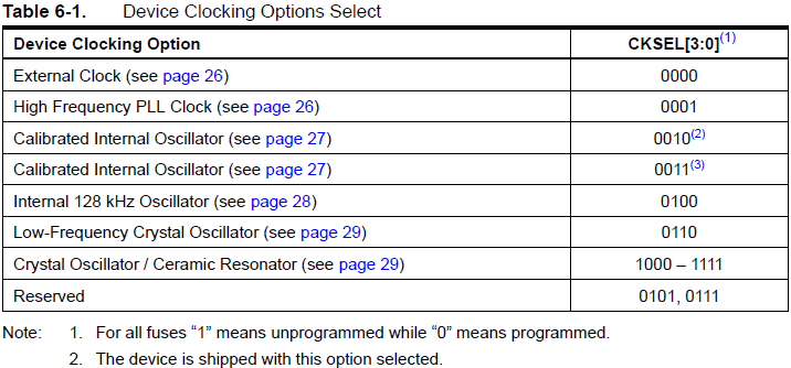
pauseSo the same procedure as before with setting the path. Then the call to avrdude is very similar except that this time we use the “-U” option with “lfuse:w:0xE2:m”. This tells avrdude that we want to write the lower fuse byte with the value of 0xE2. Now if you consult the ATTiny85 datasheet you will find a table that describes these bits, looking like this:

So by setting it to 0xE2 (binary 11100010) we disable the clock divider and select CKSEL = 0010 which is the internal 8MHz RC oscillator. There are also some other clock sources available like a 16MHz PLL that you could use if you need more speed. The code examples below, assumes an 8MHz clock, so if you want to try them out then maybe stick with the 8MHz clock for now. The datasheet provides the following clock source options:
Writing some code
Lets start by writing a program that toggles one of the pins on the ATTiny85, so we can then connect a LED and have it blink. To do this create a text file in the “src” folder called “main.c” and add the following code:
#include <xc.h>

void delay(volatile long delayTime)
{
	while (delayTime > 0)
		delayTime--;
}

void main(void)
{
	// Make PB0 an output
	DDRB |= (1 << PB0);

	while(1)
	{
		// Toggle PB0 with XOR
		PORTB ^= (1 << PB0);
		delay(50000);
	}
}
So let’s take a quick look at the code above. It starts with including the “xc.h” header which gives us access to some predefined macros for the ATTiny85. The first function is just a really simple delay function which keeps the CPU occupied by counting down from whichever value we give it. The entry point of our program is the main() function. It starts by making pin PB0 an output and then going into an infinite loop which keeps toggling the pin after some short delay.
Pin directions are set by writing to the Data Direction Register and in this case for port B, therefore the register is named DDRB. This register is located at address 0x17 for the ATTiny85 and DDRB is just a macro which points to this register. If you would lookup the macro you would find that it’s defined as:
(*(volatile uint8_t *)(0x17))Which is just a pointer to an 8 bit memory address. I think we can agree that it is much easier to just use these macros.
So when we write a 1 to any of the bits in this register the corresponding pin will become an output and if we write 0 it will become an input.
We want PB0 which corresponds to bit 1 in the register to be an output and therefore need to set it to 1. This is what the (1 << PB0) part does, PB0 is also a macro which is just set to 0. So if we take a value of 1 and shift it right by 0 places it is still 1 and that is what we want. In this case the shifting might seem a bit stupid but it makes the code more consistent and easier to read and understand.
Now we could just directly set DDRB to 1 but if we previously configured any pin directions they will be overridden. A better approach is to just use a OR operation. We OR the current register with itself and a byte which has the bits (which correspond with the pins) we want as outputs set to 1. All bits set to 0 will not override bits in the register.
If we wanted to use the same mechanism to make pins inputs we could use:
DDRB &= ~(1 << PB0);So after the pin directions in our main() function is set an infinite while loop is created. Inside this loop we write to the PORTB register and call a delay function. Writing 1 to a bit in the PORTB register will cause the output pin to go high if the corresponding bit in the DDR is set as an output (logic 1). Writing a 0 to a bit in the PORTB register will cause the output to go low.
We toggle the output to pin PB0 by performing an XOR (eXclusive OR) with 1 on itself. An exclusive OR will only output 1 if either of its two input are 1. So if the current bit for PB0 is 0 and we XOR it with 1 it becomes 1. Next time the loop passes it will XOR 1 with 1 which is 0 and so it repeats causing the pin to toggle between 0 and 1.
Between the pin toggles the delay is called, which is pretty basic and just decreases the value of 50000 that we gave it one by one. Just burning up CPU cycles to pass the time. Not very efficient but for this example it will do. So how long is this delay? The quick answer is about 208 milliseconds, I measured it with my oscilloscope.
The long answer, if you are interested, comes from a quick peek at the assembler code. After building the program (in the next section) an assembler file (.s) will also be created and if we look at the delay function we see that there are actually a whole lot of instructions involved. This is because we are using a 4 byte long variable which requires multiple instructions to perform even a simple subtraction. You can now go lookup how many cycles are required for each instruction. Since we are using a 8MHz clock we know each cycle lasts 0.125 microseconds. I made a quick rough count of the loop section and counted about 33 cycles. So 33 cycles taking 0.125us and repeated 50 000 times gives 206.25 milliseconds. But then we still need to add the overheads of the instructions before and after the loop which would bring it closer to the 208 milliseconds measured by the oscilloscope.
Building the program
We can now build our program by running the “build.bat” file we created earlier. This should generate 3 files in the “output” folder ending on .elf, .hex and .s and in die command window we should not see any error messages.
Flashing the program
Firstly we want to set the fuses on the ATTiny85, so with your programmer and ATTiny85 connected run the “writeFuses.bat” file we created earlier.
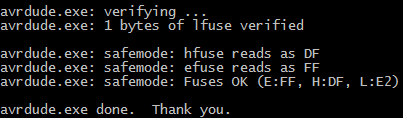
In the command window output double check that the fuses show the corrected values, should look something like this:
Now that the fuses are set we can program our code to the flash memory of the ATTiny85. Programming the ATTiny85 will not override the fuses so the above step is only required once or whenever you want to change the fuses in the future.
To program the ATTiny85, make sure the programmer is connected and run the “flash.bat” file we created previously. If all went well there should be no errors and your ATTiny85 would start running it’s newly uploaded program. If you attached a resistor and LED to PB0 then you should see it flashing rapidly.
Using Timers
Next up we will replace the delay function by using a hardware timer instead. Just in case you are not familiar with hardware timers/counters, most microcontrollers have at least a couple of them integrated. They are great for time keeping and counting purposes and can be used to relieve the CPU of these kind of tasks. For example in the code below we will tell the timer to start counting up to some value and only once it reaches this value should it interrupt the CPU. The nice thing is that while the timer is counting the CPU can do other tasks.
Lets have a look at the code:
#include <xc.h>

volatile uint16_t time_now = 0;

void __interrupt(TIM1_COMPA_vect_num) isrTim1CompA(void)
{
	TCNT1 = 0;				// Reset counter value
	time_now++;
}

void main(void)
{
	uint16_t time_delay = 0;

	// Make PB0 an output
	DDRB |= (1 << PB0);

	// Setup Timer1
	TCCR1 |= 0x04;				// Set clock prescaler to 8
	TCNT1 = 0;				// Reset counter value
	OCR1A = 100;				// Set compare register A
	TIMSK |= (1 << OCIE1A);			// Enable register A compare interrupt

	// Enable Global Interrupts
	SREG |= (1 << SREG_I);

	while(1)
	{
		if (time_now == (time_delay))
		{
			PORTB ^= (1 << PB0);	// Toggle PB0 with XOR
			time_delay = time_now + 5000;
		}
	}
}
We now have a new function called isrTim1CompA() which will handle an interrupt that is triggered by Timer1. The “__interrupt(TIM1_COMPA_vect_num)” part of the function declaration is a XC8 specifier which tells the compiler that this function will act as an interrupt handler. Note that this specifier requires the “-mext=cci” option when building, which we already included in our “build.bat” file previously.
If you look under the Interrupts section of the ATTiny85 datasheet you will find a table showing the interrupt vectors:
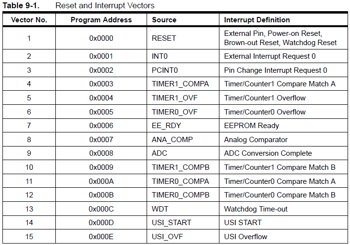
Looking at vector number 4 in the table we see that it sits at address 0x0003 and is described as “Timer/Counter1 Compare Match A”. This is the vector we want to use, why specifically this one will become clear when we look at the Timer1 setup code. The important thing for now is that this vector sits at address 0x0003 and that the “TIM1_COMPA_vect_num” part in the specifier is nothing more than a macro for this address.
So with the interrupt handler in place lets look at the setup of the timer. The ATTiny85 has 2 timers, Timer0 and Timer1, for this example I just picked Timer1. The first register that we configure is the TCCR1 (Timer Counter Control Register 1) which has the following bits:
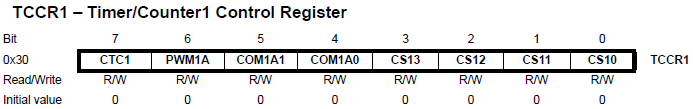
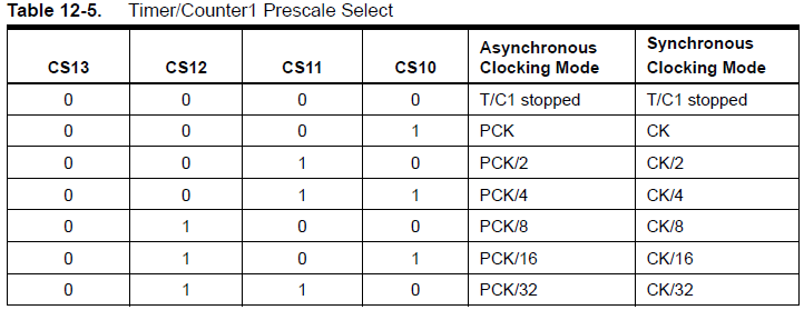
The last 4 bits (CS13, CS12, CS11 and CS10) are the ones that are important to us and is used to set the clock prescaler. In other words by how much the clock we use should be divided (scaled) first before it clocks the timer. We will use the timer in synchronous mode which means it is clocked by our 8MHz clock. In the code we set the prescaler to 0x04 which indicates that we divide by 8 (see the table below) giving a timer clock of 1MHz. So in other words the counter in our timer will increase every 1us.
Note that you can disable the timer by setting the prescaler to 0.
The next register is TCNT1 which hold the counter value that is increased on each clock cycle. All we do here is to set it to 0 so that we know where we are starting from.
Then we have the OCR1A (Output Compare Register A) register and as it’s name suggest it is used to compare it’s value to the counter (TCNT1) value. OCR1A is set to 100 meaning after 100 counts of 1us there will be a match between OCR1A and TCNT1. The action we want it to take when the comparison is a match is to trigger the interrupt we previously defined, now the “Timer/Counter1 Compare Match A” vector description we talked about earlier should make more sense. To do this we set the OCIE1A (Timer/Counter1 Output Compare Interrupt Enable) bit in the TIMSK (Timer/Counter Interrupt Mask Register) register.
That’s it the timer is all setup and ready to go, all that is left to do is to enabled interrupts globally by setting the SREG_I bit in the SREG register. So every 100 microseconds the interrupt would be triggered which just resets the TCNT1 counter value and increases the “time_now” variable by 1. We can now use the “time_now” global variable for general time keeping tasks. Note that this variable is declared with the “volatile” keyword, which is important to do for variables used inside of interrupt handlers. Since the compiler can’t predict when an interrupt will be triggered it might assume variables inside the interrupt handler function is never used and optimize them away. By using “volatile” we tell the compiler not to do so.
The code in the while loop in the main function is pretty straight forward. It toggles the PB0 pin and then adds 5000 units to the current “time_now” value, wait for it to pass and repeats the process again. Since “time_now” has a resolution of 100 microseconds (or 0.1 milliseconds) it means that PB0 will toggle every 500 milliseconds.
You can now build and flash the code above in the same way as in out first example (no need to write the fuses again). Again if you have a resistor and LED connected to PB0 it should start flashing, but this time a bit slower then in the previous example.
If we were to hook-up pin PB0 to an oscilloscope and measure the time for which PB0 is high or low we see a small error in timing. Below is a trace of the above code:

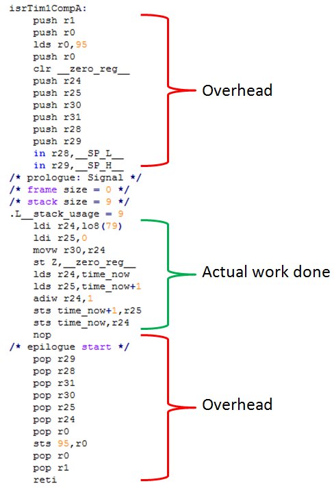
We see that PB0 is actually toggling a few milliseconds slower than what we expect. The reason for this is mostly due to the overheads of the interrupt which is triggered. When an interrupt triggers the CPU stops what it is doing and jumps to the interrupt handler function, performs the tasks in this function and then returns to what it was busy doing. In order for it to be able to return to what it was doing before the interrupt, it needs to first store all the registers values. This is normally done by pushing (writing) the register values to the stack memory before the interrupt handler code and popping (reading) them back afterwards. All this is handled by the compiler (through the __interrupt specifier) and therefore not visible to us in the code. But visible in the output as these extra instructions eat up additional cycles and time for which we did not account. If were to look at the assembly output of the code then we would clearly see the pushing and popping instructions at the start and end of the interrupt handler function.
So the bottom line is that if we want our time keeping variable to be more accurate we would need to compensate for these extra instructions. The easiest way to do this is to adjust the value in the output compare register (OCR1A). I changed the value to 97 and although not spot on, it’s for sure much closer:

Using the ADC
Incredibly enough the ATTiny85 also packs a 10bit ADC with sampling times of between 65us and 260us. It is also super easy to use and very configurable.
Let’s take a look at a simple code example and then walk through how it works:
#include <xc.h>

uint16_t adc0;

void main(void)
{
	// Make PB0 an output
	DDRB |= (1 << PB0);

	// Select Vcc Ref. + Right Adjust + PB5 (ADC0)
	ADMUX |= 0x00;

	// Enable ADC + div 64 prescaler
	ADCSRA = (1 << ADEN) | (1 << ADPS2) | (1 << ADPS1);

	while(1)
	{
		// Start conversion
		ADCSRA |= (1 << ADSC);

		// Wait for conversion to complete
		while (ADCSRA & (1 << ADSC));

		// Load the 16 bit ADC value
		adc0 = ADCH;
		adc0 = adc0 << 8;
		adc0 &= ADCL;


		if (adc0 > 512)
			PORTB &= ~(1 << PB0);
		else
			PORTB |= (1 << PB0);

	}
}
The above code reads an analog voltage on PB5 which is connected to analog channel 0 (ADC0). When the voltage is above half the supply (Vcc) voltage the output on PB0 goes low otherwise it outputs a high level.
On the very top we declare a 16 bit unsigned integer to hold the ADC reading and then the first line of our main() function makes PB0 and output.
The first ADC register we configure is ADMUX which we set to use Vcc as reference, have the reading right aligned and select channel ADC0 (pin PB5). Next we configure the ADC control register by selecting a clock prescaler and enabling the ADC.
The ATTiny85 datasheet recommend that we use a clock of between 50kHz and 200kHz for the ADC. To get this ADC clock a prescaler is provided to divide the main clock down. Since our system clock runs at 8MHz I picked the divide by 64 prescaler which gives a 125kHz ADC clock. Each conversion takes 13 ADC clock cycles to complete, except for the very first one which take 25 cycles as it also performs some initialization. So this means that we can expect a conversion to take about (125kHz / 1) * 13 = 104us.
With those two registers configured we can start a conversion by setting bit 6 (ADSC) in the ADCSRA register. Once the conversion is done this bit will be cleared so we can poll it and loop until it clears. Once the conversion is done we copy the high (ADCH) and low (ADCL) data register to our previously defined “adc0” variable. Then lastly we check if “adc0” is larger than 512 and if so clear PB0 or set it if not. This last part sits inside an infinite while loop so will keep repeating forever. Since the ADC reading = (Vin * 1024) / Vref it means that a reading of 512 will be about 2.5V if we powered the ATTiny85 from 5V.
So that is it for our ADC example but I would recommend that you check out the datasheet for more interesting features. You could for example use one of the timers to trigger measurements so that your program does not need to wait for the conversion to finish. Another nice feature is that one of the ADC channels is actually connected to an internal temperature sensor which you could read.
Writing in assembly
Well in the beginning we asked, how low can we go? So lets go one step lower as a bare metal post on the ATTiny85 would not be complete without at least a basic blink program coded in assembly language!
If you want to follow along on this example then I would suggest to also keep the AVR instruction set manual within reach. It provides you with a description of each of the instructions and in most cases also a small example on how to use it.
I don’t claim to be an expert at assembly but could muster up at least the following blink program.
I used the same folder structure as before and created a file “test.s” in the “src” folder.
.equ SPH,	0x3E				; Stack Pointer High Address
.equ SPL,	0x3D				; Stack Pointer Low Address
.equ DDRB,	0x17				; Data Direction Register PortB
.equ PORTB,	0x18				; PortB output register


.org		0x0000				; Start of program
	rjmp	0x0010				; Jump over vectors to main part

.org		0x0010				; Main part of code

	ldi 	r16, 0x02			; Setting up the stack at top of RAM
	out 	SPH, r16
	ldi 	r16, 0x5F
	out 	SPL, r16

	ldi 	r16, 0x01			; Set PB0 as output
	out	DDRB, r16

loop1:						; Outer loop
	ldi   	r25, 0xC3			; Load register pair r24 and r25
	ldi   	r24, 0x50  			; Low byte

	ldi	r16, 0x01			; Toggle PB0
	in	r17, PORTB			; Get current port bits
	eor	r17, r16			; Perform XOR
	out	PORTB, r17			; Write to PortB

loopDelay:					; Inner delay loop
	rcall	delay				; Burn some cycles
	rcall	delay
	rcall	delay

	sbiw   	r24,1				; Subtract, Z = 1 if result 0

	brne 	loopDelay 			; Branch if r17 != 0
	rjmp 	loop1				; Run outer loop


 ; Burns 10 cycles when called
 ; rcall=3 + ret=4 + nop=3
 delay:
  nop
  nop
  nop
  ret
The program starts off by defining some register names with their corresponding addresses. By doing this we can just use the register name in the code and don’t have to remember the register address.
At address 0x0000 of the program memory we place a jump instruction to address 0x0010. The reason for this is that once the ATTiny85 is powered up or reset it will start executing instructions at address 0x0000. But the first 16 addresses in the program memory can also be used for interrupt vectors and since we don’t want to write to those addresses we jump 16 addresses further. The ATTiny85 datasheet states that if you will never use interrupts then you could actually use these addresses. I just thought it would be good practice to jump over them anyway.
Okay, so after the jump the first thing we need to do is initialize the stack pointer. I assume you are somewhat familiar with how stack memory work but just to recap. It is basically just a first in last out buffer, so we write data by pushing it to the stack and read it back by popping it from the stack. This mechanism is used by some instructions and therefore the sooner we initialize the stack pointer the better. The initialization is as easy as just specifying an address in SRAM memory where the top of the stack memory will be. This address is then loaded to the stack pointer register, in most cases the last address in the SRAM is used as the top of the stack. This is because each time you push data to the stack the stack pointer is decreased, so it grows downwards. So therefore the stack pointer register pair is loaded with the value 0x025F which is the last RAM address for the ATTiny85.
With the stack pointer initialized we set bit 1 of the data direction register to make PB0 and output.
Next we start with the pin PB0 toggle and delay loop. The delay will be created by running a loop of NOP (No OPeration) instructions which just eats up cycles and time. One problem though is that we would need to run a good number of loops to make up enough time and an 8 bit register (counting up to 255) will just not be enough. Luckily some registers can be used in pairs to form a 16 bit register and one of these pairs are r24 and r25. So the loop is formed by loading a value to these registers and then using instruction “sbiw r24,1” to subtract 1 from the register pair. If after the subtraction the result is 0 then the Z flag will be set, instruction “brne loopDelay” will test for the Z flag and if not set jump to the “loopDelay” label. In case it is set (meaning that the r24 and r25 register pair equals 0) it will continue to the next instruction which is a jump to “loop1” label. Here the r24 and r25 register pair will be loaded again and pin PB0 toggled by performing an exclusive OR on itself and the value 1.
So to build the assembler code we can create another “buildAsm.bat” file with the following contents:
SET PATH=%PATH%;E:\Programs\Microchip\xc8\v2.31\bin
CLS

xc8-cc.exe -mcpu=attiny85 -nostartfiles -o output\test.elf src\test.s
avr-objcopy.exe -O ihex output\test.elf output\test.hex

pause
The difference in this file from the previous “build.bat” file is the options we use with “xc8-cc.exe”. The first thing that changed is the source is now the “test.s” assembler file. The second difference is the -nostartfiles option. When compiling C code the compiler uses a default start file which performs some initialization like setting the stack pointer and copying some values around before calling the main() function. In our assembler code we don’t want this as we don’t have a main() function and will be handling everything ourselves. So therefore this option is used to tell the compiler to not use the default start file.
To flash the program you can just use the same “flash.bat” file we created previously.
If you want to experiment a bit more with coding in assembler might I also suggest you try out this AVR simulator. It provides a very nice visual overview of the registers and memory and allow you to step through instructions. This way you can easily test your program before uploading it.
Program Sizes
So now having written a blink program in a couple of different ways, I thought it might be interesting to compare them in terms of program and RAM size. Below is a table of how they stack up against each other:
| Code | Flash Memory | RAM |
| Normal Arduino Blink Example Code | 684 bytes (8.3%) | 9 bytes (1.8%) |
| First blink example in this post | 186 bytes (2.3%) | 0 bytes (0%) |
| Blink using the Timer | 358 bytes (4.4%) | 2 bytes (0.4%) |
| Blink using assembly without Timer | 60 bytes (0.73%) | 0 bytes (0%) |
I used the “avr-size.exe” on the .hex files to determine the amount of program memory they will use. For the RAM I did the same but using the .elf file and looking at the data section. The Arduino compiler had “-Os” optimization enabled to produce the smallest possible output, but then again I am not sure how much that would really help for such a small program.
Would not say that I expected a much different result. We know that the Arduino libraries have to cater for a lot of different hardware and therefore have some overheads that one have to live with. The Timer code took up a bit more space then I thought but can be explained by the overheads added by the interrupt context saving code. And then obviously the pure assembler version takes the lead by far, only 60 bytes! I am sure somebody with skills can bring this down even more.
The ATTiny85 only has 8192 bytes of flash memory and 512 bytes of RAM. So if you look at the difference between using bare metal C and using Arduino it might just be worth your time to use only C on this tiny device.
So there you have it, the basics of going bare metal on the ATTiny85. Hope you could find something useful in here for your next project or at least learn something new.